
Engineering Ceramic Co.,( EC © ™) Report:


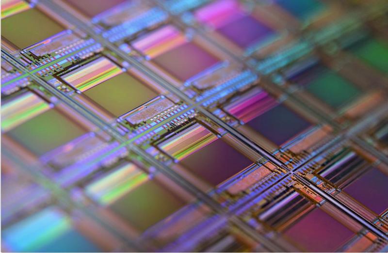
Silicon carbide (SiC), as the third generation semiconductor material, has become an important development direction of semiconductor material technology due to its excellent properties such as wide band gap, high breakdown electric field strength and high thermal conductivity. In the semiconductor industry chain, silicon carbide lining Silicon carbide is the basic material for wafer manufacturing, and quality inspection of silicon carbide wafer materials is a key link to ensure performance. In China’s semiconductor industry, commonly used detection technologies for silicon carbide single crystal substrates include:
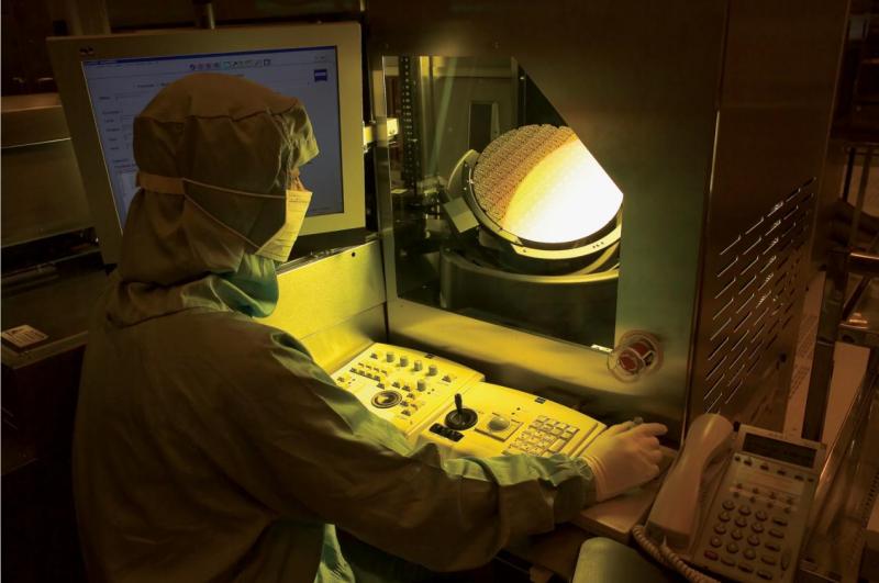
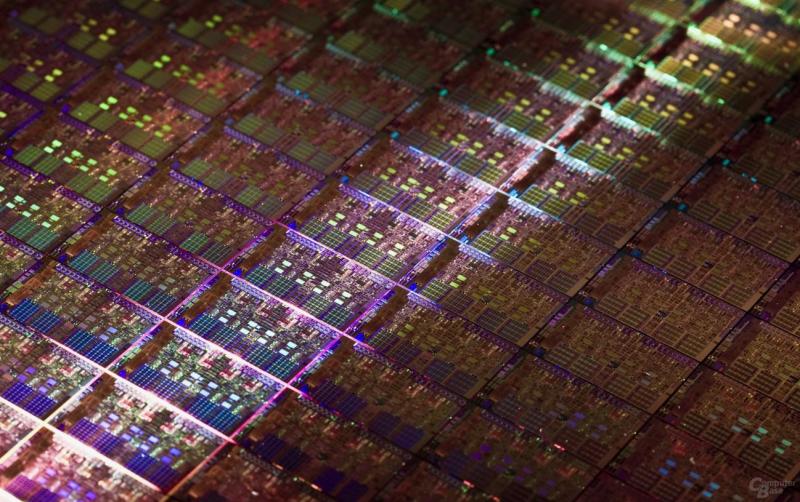
I. Geometric parameters
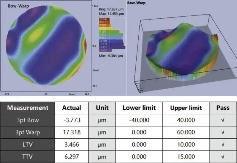
Thickness
Total Thickness Variation, TTV
Bow
Warp
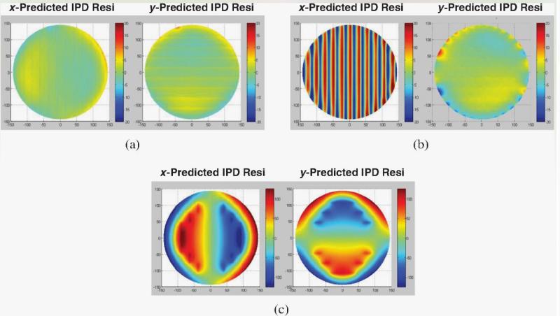
The following test report comes from Corning Tropel® FlatMaster® FM200 Fully-Automated Wafer System, this equipment is currently widely used in China.

II. Defect
In silicon carbide single crystal substrate materials, defects are usually divided into two major categories: crystal defects and surface defects.
Point Defects - PD
Micropipe Defects - MP
Basal Plane Dislocations - BPD
Edge Dislocations - TED
Stacking Faults - SF
Screw Dislocations - TSD

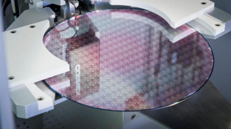
Technologies for detecting surface defects mainly include
Scanning Dlectron Microscope - SEM
Optical Microscope
Cathodoluminescence - CL)
Differential Interference Contrast - DIC
Photo Luminescence - PL
X-Ray Topography - XRT
Optical Coherence Tomograph - OCT
Raman Spectroscopy - RS


Statement: The article/news/video is from the Internet. Our website reprints for the purpose of sharing. The copyright of the reprinted article/news/video belongs to the original author or the original official account. If there is any infringement involved, please inform us in time, and we will verify and delete it.